1) Title Page The title page should include your name, experiment number and title, lab partner name, and the date the lab was performed.2) IntroductionThis section should include a brief overview of
 Lane Department of Computer Science and Electrical Engineering
Lab: 1
CpE 272 Digital Logic Laboratory
Basic Logic Gates and Seven Segment Displays
Spring 2017
West Virginia University - College of Engineering and Mineral Resources
Basic Logic Gates
The basic building blocks of any digital system are logic gates. These are simple elements with two or more inputs and one output. The outputs of the logic gates depend on the values of the inputs. In the digital world we always have two possible values for each input or outputs. When it comes to the theory, we represent these two values by “logic high” or “logic low”
( “1” or “0” / “true” or “false” represent the same)
When it comes to the real circuits, which operate on electricity, two distinct voltage levels are used to distinguish between these two logic levels. i.e. +5V to represent the logic high and 0V to represent the logic low.
There are 4 different basic logic gates: AND gate, OR gate, XOR gate and NOT gate.
Derived from these basic logic gates a NAND gate, NOR gate and XNOR gate can be made by connecting a NOT gate to the outputs of AND, OR and XOR gates.
The bubble at the output node represents this NOT operation. Altogether there are 7 logic gates and each gate has its own symbol as shown in Figure 1.
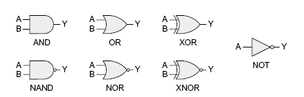
Figure 1: Logic Gate Symbols
Truth tables are often used to illustrate logical relationships as shown for the AND operation in Table 1.

Table 1: AND Gate Truth Table
A truth table provides a direct mapping between the possible inputs and outputs. A basic AND operation has two inputs with four possible combinations, because each input can be either a 1 or 0 — true or false.
Logic Integrated Circuits (ICs)
Depending on the circuit technology being used, there are different kinds of logic families. They are CMOS, TTL and ECL. The difference is mainly with the operating speed and the supply voltage required to power up.
True = One = High For TTL > 2.4V
False = Zero = Low For TTL < 0.8V


Figure 2: Integrated Circuit in dual inline package
Figure 3: AND Gate Internal Connection Diagram
The 74LS08 IC chip is a quad AND gate. As illustrated in Figure 3, the chip has 4 AND gates connected to 12 pins of the chip. It also has two pins labeled Vcc and GND to supply the power. The Vcc pin needs to be hooked up to +5v supply while the GND pin needs to be grounded. Note the semi-circle notch in Figure 3 that differentiates the different ends of the chip and helps when one is wiring it.
Goals of this Lab
This is an introduction to basic concepts of logic gates, and familiarization with some lab tools. We will be working with integrated circuit chips (ICs).
Here are a few rules to follow:
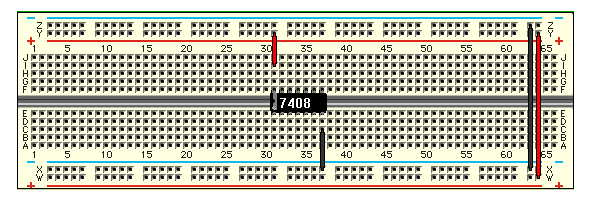
Connect a wire from the +5 volts to the bus with a red line and a wire from ground to the bus with a blue line. This will now allow you to have a more organized proto board.
Be careful to avoid reversing power connections. Typically we only need +5 V and 0 V (ground) connections for digital circuits. Ask your Teaching Assistant for help with setting up power busses on your prototype board if in doubt.
When placing your chips have them lay over the large gap in the middle of the proto board.


All the slots in each column are connected together
Figure 4: AND Gate Proto-Board Setup
Make sure to connect the Vcc pin (Pin 14) to +5V volts and the ground pin (Pin 7) to ground for every chip!
We will primarily be using TTL circuitry. Do not connect TTL outputs together; as the resulting circuit will not work (multiple inputs can be connected).
It is a good convention to have all your chips oriented in the same direction. For example have all the semi-circle notches pointing one direction.
Verification of IC Chips
Verification: Verify that the AND, OR, NOT, XOR, NAND, NOR, and XNOR IC chips operate correctly by determining their truth tables on the proto-board. When doing this connect the two inputs to two pushbuttons and the output to a LED.
AND Gate - The logic expression for the AND operation is given by
Y = AB
Or
Y = A . B
In this part you are going to verify the truth table by wiring a 74LS08 IC on the proto-board. The internal connection diagram of the 74LS08 IC chip is shown in Figure 4 along with its corresponding truth table in Table 2.
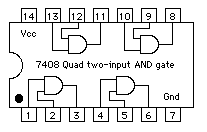
Table 2: AND Gate Truth Table
Figure 4: AND Gate Internal connection Diagram
| Inputs | Output | |
| A | B | Y |
OR Gate - The logic expression for the OR operation is given by
Y = A + B
In this part you are going to verify the truth table by wiring a 74LS32 IC on the proto-board. The internal connection diagram of 74LS32 IC chip is shown in Figure 5 along with its corresponding truth table in Table 3.
Table 3: OR Gate Truth Table
| Inputs | Output | |
| A | B | Y |
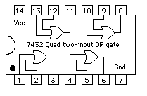
Figure 5: OR Gate Internal Connection Diagram
NOT Gate - The logic expression for the NOT operation is given by

Y = A
In this part you are going to verify the truth table by wiring a 74LS04 IC chip on a proto-board. The internal connection diagram of 74LS04 is given in Figure 6 along with its corresponding truth table in Table 4.
Table 4: Not Gate Truth Table
| Input | Output |
| A | Y |
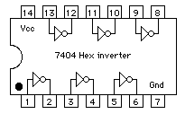
Figure 6: NOT Gate Internal Connection Diagram
NAND Gate - The logic expression for the NAND operation is given by
Y = (AB)’ or Y = (A.B)’
In this part you are going to verify the truth table by wiring a 74LS00 IC chip on a proto-board. The internal connection diagram of 74LS00 is given in Figure 7 along with its corresponding truth table in Table 5.
Table 5: NAND Gate Truth Table
| Inputs | Output | |
| A | B | Y |

Figure 5: NAND Gate Internal Connection Diagram
XOR Gate - The logic expression for XOR operation is given by

Y = A + B
In this part you are going to verify the truth table by wiring a 74LS86 IC chip to a proto-board. The internal connection diagram of 74LS86 is given in Figure 8 along with its corresponding truth table in Table 6.
Table 6: XOR Gate Truth Table
| Inputs | Output | |
| A | B | Y |
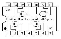
Figure 8: XOR Gate Internal Connection Diagram
Part I – Building Logic Diagram Circuits
 In this part you are going to wire the following logic diagrams on the proto-board and determine each ones truth table by using pushbuttons to enter different input combinations.
This is the information you want in your Experiment section.
Experiment 1:
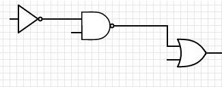
G3
G2
G1
Y
C
B
A
Logic Expression (i.e. the equation for Y): __________________________________________________________
This is the information you want in your Results section.
| A | B | C | G1= | G2= | G3=Y= | |
NOTE: In lab report make sure to include logic diagram, logic expression, and the output truth table.
Experiment 2:

This is the information you want in your Experiment section.
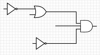
G4
G3
G2
G1
C
C
Y
B
A
Logic Expression: __________________________________________________________
This is the information you want in your Results section.
| A | B | C | G1= | G2= | G3= | G4=Y= |
NOTE: In lab report make sure to include logic diagram, logic expression, and the output truth table.
Part II- Combinational Logic Networks
The logic gates explained earlier can be connected to make useful decision making systems. Those circuits are called combinational logic networks. The output of those circuits depends on the inputs and the function it performs.
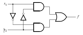
As a design example, we will design a two-way light controller circuit. The circuit can be used to control a single light from either of the two switches, x1 and x2, where a closed switch corresponds to the logic value 1. Figure 9 shows the truth table of the circuit.

Figure 9: Two-way Light Controller Truth Table
We can write a Boolean equation for any truth table by summing each of the minterms for which the output, f, is TRUE.
NOTE: A minterm is a product involving all of the inputs to the function. A.B.C is a minterm for a function of the three variables A, B, and C, but A.B is not, because it does not involve C. When creating a minterm the inputs that are logic low are complimented in the expression.
For example, in Figure 10, there are only two rows (or minterms) for which the output f is TRUE (logic high), shown circled. Looking at these two rows, use AND gates to sum the inputs and then an OR gate to connect the two terms together. Lastly, complement each input that is logic low.

Figure 10: Circled Minterms
Resulting Logic Expression using Minterms:
Once the logic expression is found the logic gates can be used to realize the function. In this case,
In your Experiment section, very briefly explain minterms concept. Then, explain what is being asked of you to be solved.
If you remember the XOR function, this performs the same operation.
 Experiment: Three inputs can be used to represent the numbers 0 to 7. If you have A,B,C lines (inputs) which represent a number, design a circuit to find whether the number it represent is divisible by 3. Thus, the output of the circuit should be high whenever the input represents a number divisible by 3 (Do NOT include zero as divisible by 3).
| Binary | Decimal | |||

Come up with a truth table to accomplish this task.
Truth Table:
| Decimal | Binary | Y | |||
Results section material
Derive the logic expression using minterms.
Logic Expression: ___________________________________________________________________
Algebraically minimize the above expression:__________________________________

Draw the circuit diagram according to the algebraically minimized expresion and construct the circuit on the proto-board. Demonstrate this to your instructor.
Circuit Diagram:
Results section material
NOTE: In lab report make sure to include truth table, logic expression, and the circuit diagram (or logic diagram).
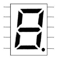
Seven Segment Displays
Seven-Segment displays use 8 LED’s to display numbers and characters by lighting in any desired combination. These displays require drivers or decoders that must be either purchased as chips or designed. To light up a segment in a seven segment display, a logic low must be supplied to the corresponding segment if you are using a common anode type display.
The term "common anode" refers to the fact that the anode portions of each LED segment are connected together at the upper voltage source. This means that individual LED segments are lit by connecting their cathode to a lower voltage. Although it seems backwards to turn on the LED segments with a low signal, early logic chips like standard TTL are capable of delivering a greater amount of current with an output that is logic low.
Experiment Section
Part III – Seven Segment Display
All components are represented by a part number which can be used to look up its corresponding datasheet. A datasheet contains all kinds of information about a specific device such as the driving current, operating temperature range, pin connections, etc.
Using the internet and the part number, which can be found on the component, look up the datasheet for the common anode seven segment displays. With the aid of the datasheet, correspond letters a through g on the segments below to its respective pin. Segments a , d, and pin 1 are already given as a good starting reference.

Common
anode
d
a
10
9
8
7
6
5
4
3
2
1
d
a
Results Section
Common Anode Seven Segment Display
Have your TA check the diagram you have created and place this diagram in your report.
Place both a seven segment display and resistor on a proto-board. Connect +5V through the resistor pack and then into the seven segment display. Display the number 5 on the 7-Segment display by hardwiring the correct segments to ground.
Note: In the lab report make sure to include the completed 7-segment display and explain how you accomplished getting the number five to light up.
Post-lab Questions for Lab 1:Draw a truth table (similar to the last experiment) to represent number 0-7 divisible by 2. Again, don’t include zero. Find the output minterm logic expression.
Draw a logic diagram to show how you could construct an AND gate using only NAND gates. Label your inputs and outputs
Comparing the two expressions of the divisible by 3 experiment (i.e. Part II: 2a and 2b), what was the overall benefit of manipulating the expression if they both give you the same exact output and why the effort was useful? (HINT: Think about if you were given a choice to construct one the expressions into a breadboard circuit. Which one would you choose and why?)
When using a common anode seven segment display, does applying a logic high or logic low signal light up a segment? Why does it function that way or why wouldn’t it be the opposite logic signal of what you stated?
What is a binary subtractor?


