VHDL CODE for RAM Implementation of Hack Computer
RAM subsystems Block Level Diagram and Description for VHDL Hack Computer using an FPGA device
Introduction
A computer has many different kinds of memory that are used to hold data and programs. Random access memory (RAM) is a type of computer memory that is volatile and it is used to hold computer instructions just before and immediately after processing. It is referred to as random because the time it takes to access any piece of data is independent of the data’s physical location. In other words it can access data at an address directly without sequentially looking at each address location to find a specific piece of data.
A computer is supposed to carryout complex arithmetic computation in the CPU. Registers, although fast, can only store a few instructions. RAM has a large amount of memory compared to CPU registers, this enables them to store a lot of information that has just been processed or that is yet to be processed.
Overarching Hack Computer Design Diagram
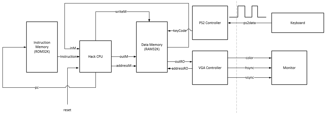
Computer RAM Architecture
A RAM block is composed of smaller RAM chips, or memory mapped I/O devices. The registers store the data to be used and the direct access logic unit provides the logic to search for the needed data.

Our RAM design has four (4) inputs, a clock signal, and two (2) outputs. The four (4) inputs are rw_load input that selects whether the operation will be read or write, a write data input, an address input from the CPU, and a read only address input from the VGA controller. The rw_clock signal syncs the timing for all read and write inputs and outputs and the ro_clock syncs the timing for the VGA controller read operations. One output is a read only for the VGA controller. The other output feeds the input of the hack CPU. The multiple inputs and outputs could be accomplished using the True dual-port RAM mode.
True dual-port RAM allows the following features
• Simultaneous two reads.
• Simultaneous two writes.
• Simultaneous one read and one write at two different clock frequencies.
So in reality, there will need to be an additional load input (ro_load) and a data input (ro_data) within the RAM subsystem to accommodate the VGA controller.

In the case of a read operation (rw_load = 0), the RAM’s output immediately emits the value of the selected register.
In the case of a write operation (rw_load = 1), the selected memory register commits to the input value in the next time unit, at which point the RAM’s output will start emitting it.
The basic design parameters of a RAM device are its data width—the width of each one of its words, and its size—the number of words in the RAM. Modern computers typically employ 32- or 64-bit-wide RAMs whose sizes are up to hundreds of millions.
Our RAM configuration consists of:
rw_data – incoming data to be written.
rw_address - specifies the address or location to read from or write to.
ro_address - specifies the address or location to give to the VGA controller.
rw_load - selects between reading from, or writing to the memory.
rw_out – outgoing data to be read by the CPU.
ro_out – outgoing data to be read by the VGA controller.
RAM OPERATIONS:
Read Operation
One of the basic operations on a RAM is to read or get stored information. The following steps need to be performed during a read operation from RAM:
Select the read operation by ensuring the “rw_load” is set to 0.
Send the desired address to the address input
The contents of that address appear on the appropriate “out” (rw_out or ro_out) after a little while.
In the read operation, the “rw_data” input is not used for read operations.
Write Operation
Another important function of the RAM is to write or store information. This can be achieved by the write operation. Here are the necessary steps involved.
Write operation is selected by setting rw_load = 1.
Send the address where data/word is to be written to the address input.
Word to be stored is sent to the “rw_data” input.


