This is for a digital logic course. I need the desired outcome in the attached assignment (this will further be implemented into a 0-59 counter in vivado).
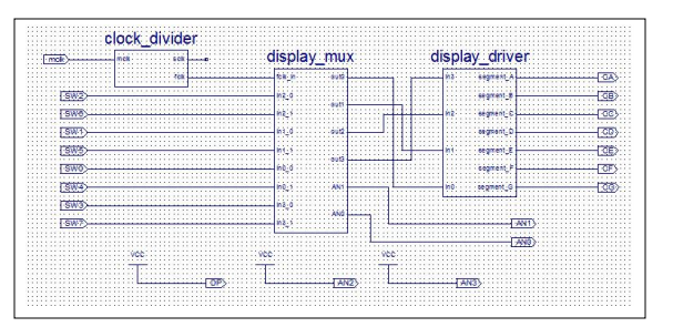
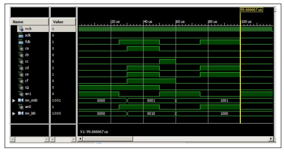
Lab 9 Assignment All work signed off or turned in for this lab must be pledged as the work of you and your lab partner ONLY – each student must do their own simulations and turn in their own signoff sheet. Prelab Assignment: In this assignment, you will create a system that will display the 4-bit binary number from switches SW0-SW3 on the right most digit display, and the 4-bit binary number from the switches SW4-SW7 on the next digit to the left. To do this, the system must output the proper values on the cathode connections (i.e., CA, CB, CC, etc.) for the given digit at the same time as the proper anode connection (i.e., AN0, AN1, AN2, AN3) for a short period of time, and then switch to the next digit. This relationship is shown in the figure below. For this system, you will use the display driver for the 7-segment display that you developed in lab8 to output the values for the cathode connections. You will only need one of these connected to the 7-segment display component. On the inputs to the display driver, you will need a multiplexor component to select the proper inputs, either SW0-SW3 or SW4-SW7 to the display driver to correspond to the proper digit being lit. You will also need to assert the anode connections, AN0, and AN1, in concert with the corresponding digit inputs to the display driver. 1. Open your lab8 project and use the Copy Project menu item to create a copy of the project called lab9. This will make it much easier to reuse the 7-segment display driver you designed for lab 8. 2. Design a 4-input, 2-to-1 multiplexor component. The inputs should connect to the SW0-SW3 and SW4-SW7 signals and the outputs should connect to the inputs of the display driver component. Add the clock divider to the schematic as well. The FCLK output of the clock divider should drive the select input of the 2-to-1 mux. The multiplexor component should also drive the AN0 and AN1 signals as required to select the correct digit to be lit. The schematic should look like the one below. 3 3. Simulate the circuit to insure proper operation. Your simulation results should look like those below. 4. Note that you should modify the clock divider VHDL before simulation to comment out the DIVISOR and DIVISOR2 generics for synthesis and uncomment the same generics for simulation. This will reduce the amount of time you will need to simulate the system to get the proper number of transitions on FCLK to test your system. 5. Show your prelab schematic and simulation results to the TA at the beginning of the lab and have them sign them off as correct. Keep these to include in your final report writeup.