electronic lab report with multisim
Final Project: Operational Amplifier Design
ENEE 3517-001 Electronics Lab April 28th 2016Introduction
The objective of this project is to design, simulate, and build an operational amplifier (op-amp) using only resistors, bipolar junction transistors (BJTs), and metal oxide semiconductor field effect transistors (MOSFETs), no capacitors or pre-build op-amps are allowed. This op-amp is expected to produce a very high voltage gain and have a DC offset of 0V (or at least as close to 0V as possible). After we designed the op-amp on paper to make sure it had the parameters we wanted, we simulated the design on circuit analyses software, and then we finally built the physical circuit on a breadboard.
Theory
Op-amps are able to take in positive and negative inputs and amplify them. They are also powered by two DC inputs which can determine the limits of how large the output voltage can be. Through this class and this project we learn that an op-amp is simply made up of differential amplifiers which take in the positive and negative inputs mentioned previously as well as current mirror (or current steering circuit) to bias the circuit, and typically other stages of either BJT or MOSFET transistors which accomplish a number of things such as increasing total gain or decreasing output resistance. The following is an example from the textbook of a classic Fairchild µA741 op-amp schematic which shows the multiple stages, transistors, differential amplifiers, etc.:


Fig. 1: Schematic of the classic Fairchild µA741 op-amp
The schematic shows the differential input terminals (enclosed in the rectangles) and the output terminal (enclosed in the triangle). The input stage consists of the differential amplifier which takes in and amplifies the difference between the two inputs, as well as a buffered current mirror which acts as an active load and biases the op-amp circuit. The second stage includes two emitter followers, a common-emitter amplifier, and a current source which increase the total gain and amplify the voltage further. The final stage, the output stage, consists of several transistors that work to push and output the amplified voltage.
Equipment Used
Breadboard
1 KΩ resistor (1)
Potentiometer
Npn BJT (4)
Pnp BJT (2)
Copper wire
Function generator
DC power supplies (2)
Tektronix DMM 4020 5-1/2 Fluke Digital Multimeter
TBS 1022 Tektronix Oscilloscope
Procedure
To begin this project, we started off by reviewing the textbook and our notes to brush up on op-amp design. From there we looked at several examples from our class notes and textbook, including the Fairchild op-amp discussed above, and tested them to see which we felt fit our needs the best. We finally settled on the following design:
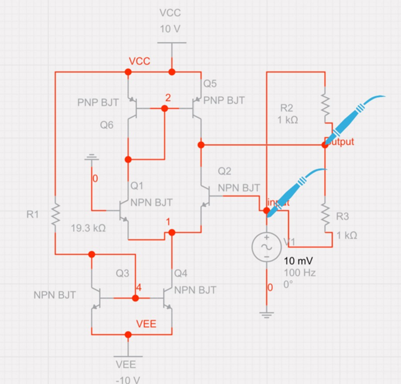
Fig. 2: Our final op-amp schematic built in Multisim Touch
Next, we assumed values for VEE and VCC which we thought would work best for our needs. From there, we assumed all transistors were in active, which is the mode BJTs must be in to act as amplifiers, and performed some DC analysis on the circuit, assuming the output and two inputs were equal to 0V. We used these assumptions to find values for the resistors and checked the conditions for active mode at each BJT, which will be found in the Calculations section. Once the circuit was designed on paper and built in Multisim Touch, we used the program to check the output and input signals, which can be found in the Results section. Finally, once everything was tested virtually, we built the physical circuit on a breadboard to see if everything worked as expected.
Measured Data
(See Results section)
Calculations
Q6
Q4
Q3
Q5
Q2
Q1
The following justifications of active mode are based on the above schematic:
Q1:
VC = VB
So active mode is confirmed.
Q2:
In DC, both differential inputs are equal 0V, SO VB4 = 0V. VB4 – 0.7v = -0.7V = VE4 = VC2. VB2 = -10v + 0.7V = -9.3V.
So, VC2 = -0.7V, VB2 = -9.3V, VE2 = -10V
VC2 > VB2 > VE2
So active mode is confirmed.
Q5:
VC = VB
So active mode is confirmed.
Q6:
VE6 = 10V, VB6 = 10V + 0.7V = 10.7V, VC6 = 0V (again, because AC sources become 0V)
VB6 > VC6
For pnp BJT, active mode is confirmed.
Q4:
VC4 = 0V, VB4 = 0
VC4 = VB4
So active mode is confirmed (similar to if they were connected)
Q3:
VB5 = VB6 10.7V = VC3, VB3 = 0V
VE3 = VB3 – 0.7 = 0 – 0.7V = -0.7V
VC3 > VB3 > VE3
So, active mode confirmed.
Results

Fig. 3: Output signal (green) vs. input signal (red) of inverting op-amp (R2 = 1k)

Fig. 4: Output signal (green) vs. input signal (red) of inverting op-amp (R2 = 50k)

Fig. 5: Output signal (green) vs. input signal (red) of non-inverting op-amp (R2 = 1k)

Fig. 6: Output signal (green) vs. input signal (red) of non-inverting op-amp (R2 = 50k)
Simulation

Fig. 7: Inverting Op-Amp in Multisim Touch

Fig. 8:Non-Inverting Op-Amp in Multisim Touch
Conclusion
The 3-staged op-amp we designed has a max gain of about 20V/V. If we decrease the R1 resistor value, the max gain value will increase. Furthermore, we found that if the input voltage is less than 5 mV or more than 1 V, the op-amp circuit acts weird and the output isn’t exact. Also, when the input(s) equal zero, the output equals 357.4 mV, ideally we want this value to be zero, but this value may be the consequence of our feedback being incorrect. We were not sure how to connect the feedback resistor to the circuit, but we connected it to the positive input voltage which resulted in a small offset. Overall, the circuit does amplify an input voltage, but only for a certain range on input voltages. We definitely learned a lot about this circuit and feel more comfortable about op-amp circuits using only differential components.


