please could you help me with my electronic lab?thanks
EENG 4109
Electronics I Laboratory
Simulation of the two-stage CMOS operational amplifier
This laboratory’s goals are to construct and evaluate the electrical performance of a simple two-stage CMOS op amp.
Notes:
A microammeter or milliammeter is represented in Multim by a series connection of a 0V voltage source and a resistance that represents the current-sense resistance of the physical device.
There are circumstances in simulation in which we will want to temporarily connect two distinct circuit nodes or connect a node to ground. Connecting two circuit nodes with wire in Multim will result in the merging of the two nets. This can be avoided by joining connected nodes through very small resistors (e.g., 0.001Ω).
Words in bold in this procedure mean that written records are required of certain specified measurements.
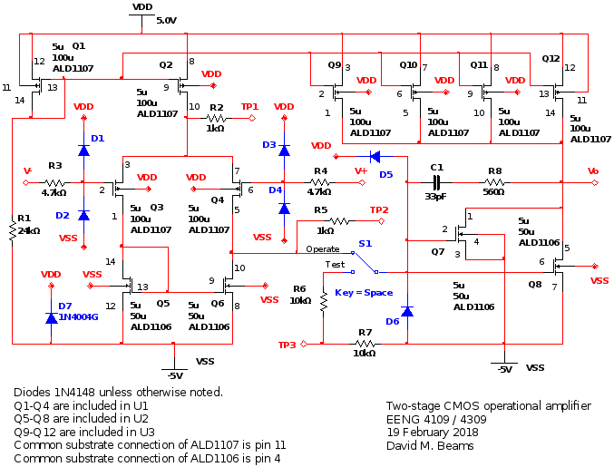
A schematic diagram of the complete op amp is attached to this procedure. Diodes in the schematic diagram are for protective purposes only and may be omitted from simulations.
Bias circuits
Begin your schematic diagram with the bias circuits. This consists of six transistors -- the diode-connected reference transistor (Q1), the current source for the differential pair (Q2), and the current source for the common-source amplifier (Q9-Q12). The bias circuits include resistors R1, R2, and test point TP1. Temporarily short-circuit TP1 and output voltage Vo to ground through simulated microammeters and measure the drain current of Q1 and the currents flowing from TP1 and Vo.
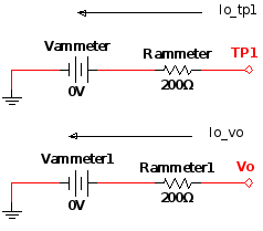
Fig. 1. Test components to add to the circuit for testing the bias network. Output currents from TP1 and Vo are read as I(Vammeter) and I(Vammeter1), respectively. The resistors Rammeter and Rammeter1 simulate the resistive loading effects of an actual microammeter.
Transconductance of actively-loaded differential pair
Add the differential pair and current-mirror load to the circuit. This comprises differential pair Q3 and Q4 and NMOS current mirror Q5 and Q6 as well as resistor R5 and test point TP2. Resistors R3 and R4 are part of protection circuits for the gates of Q3 and Q4 and may be omitted from this simulation.
Connect a differential input voltage source and set it to 0V. Attach a voltage source to TP2 and adjust its voltage until the current flowing through it is zero. Measure the voltage at TP2 (designated V(TP2)—note that it is the opposite of the voltage of source VTP2).
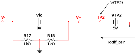
Fig. 2. Test components to be added for measurement of the output current vs. differential-input voltage characteristics of the actively-loaded differential pair. The use of two equal-valued resistors with voltage source Vid means that Vid will appear to the circuit under test as ±Vid / 2.
Note that V(TP2), the voltage at TP2, is opposite the value of test source VTP2 due to the polarity of VTP2. The polarity of VTP2 is chosen so that Multisim will give a positive value of Iodiff_pair when current is flowing in the direction indicated.
Produce a graph of the output current Iodiff_pair vs. differential-input voltage Vid over the range of -2V ≤ Vid ≤ +2V and measure the simulated value of transconductance about Vid = 0.
Output resistance of actively-loaded differential pair
Set Vid = 0V.
Set V(TP2) to 0.1V above the value that produced Iodiff_pair = 0 in Step 2. (This means decreasing VTP2 by 0.1V). Measure both the new value of V(TP2) and the current Iodiff_pair.
Set V(TP2) to 0.1V below the value that produced Iodiff_pair =0 in Step 2. Measure both the new value of V(TP2) and current Iodiff_pair.
Compute the output conductance ΔIodiff_pair / ΔV(TP2). Take the reciprocal of this value and subtract the resistance of R5 to compute the output resistance of the differential pair. Use the transconductance and output resistance of the differential pair to compute the expected voltage gain of the differential pair.
Transconductance of the common-source amplifier
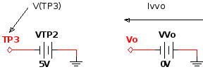
Add the common-source amplifier transistors Q7 and Q8. Also add TP3, S1, R6, R7, R8, and C1.
Place S1 in the “Test” position. Connect a voltage source VTP3 to test point TP3. Connect a 0V dc source (Vvo) to Vo. Adjust source VTP3 until the current Ivvo goes to zero. Measure the voltage V(TP3) at this point.
Set V(TP3) to 0.1V above the value that produced Ivvo = 0. Measure both V(TP3) and Ivvo at this new voltage.
Set V(TP3) to 0.1V below the value that produced Ivvo = 0. Measure both V(TP3) and Ivvo at this new voltage.
Compute the transconductance of the output stage as ΔIvvo / ΔV(TP3).
Output resistance of the common-source amplifier
Set V(TP3) to the value from Step 4 that produced Ivvo = 0. Vary V(TP3) in steps of ±0.25V about this voltage; measure both V(TP3) and the new values of Ivvo. Compute the output resistance from these data. Compute the expected voltage gain of the output stage and the expected voltage gain of the complete amplifier.
Move switch S1 to “Operate.” Configure the amplifier as a voltage follower by connecting the inverting input (V-) and the output voltage (Vo) through a very small resistance. Connect a ±1V, 1kHz pulsed voltage source to the noninverting input. Perform a transient analysis and measure both the positive-going and negative-going slew rates. External connections are shown in Fig. 4.
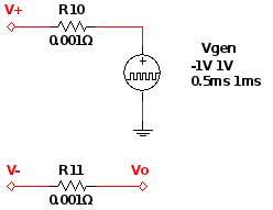
Fig. 4. Connections of the op amp as a voltage follower driven by a 1kHz pulsed voltage source.
Replace the pulsed voltage source of Fig. 4 by an ac voltage source and print a Bode plot of the open-loop gain vs. frequency characteristic of the op amp. Measure the dc open-loop gain and the gain-bandwidth product of the simulated op amp.
![]()


