Waiting for answer This question has not been answered yet. You can hire a professional tutor to get the answer.
Half-Wave and Full-Wave Rectifier
Introduction:
Week 2 lab is based on half-wave and full-wave rectifiers. Rectifiers are widely used in power supplies to provide the required DC voltage.
Please review the following videos before getting started with this lab:
- Watch the video: “Video 3: Basic Electrical Components”
- Watch the video: “Video 4: Fundamentals of breadboard”
- Watch the video: “Video 5: Simple resistive circuit with NI myDAQ”
Materials and Equipment:
Materials:
- Simulated Parts (Multisim):
- 30/3 Vrms center-tapped transformer
- Two diodes 1N4001
- Two 2.2 kΩ resistors
- One 100 μF, 50 V electrolytic capacitor
- One fuse (any rating is fine since it is for simulation only)
- Hardware Parts (In the Toolbox):
- Two diodes 1N4001
- Two 2.2 kΩ resistors
- One 100 μF, 50 V electrolytic capacitor
Equipment:
- Virtual Instruments (Multisim):
- Agilent Function Generator
- Tektronix oscilloscope
- Hardware Equipment:
- Breadboard
- NI myDAQ Instrument Device
- Screw Driver
- Screw Terminal connector
- Jumper wires
- Oscilloscope and Function generator from NI ELVISmx Intrument Launcher
Procedure:
***** This lab has to be implemented in both software (running simulations on Multisim) and hardware (using NI myDAQ) *****
Part A: Half wave rectification:
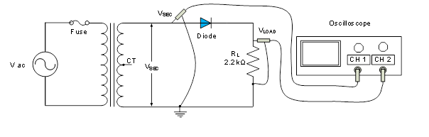
Figure 1
Software (Multisim):
- Construct the circuit of a half-wave rectifier in Figure 1 in Multisim. Use a function generator to provide the AC input of Vacand use a center tapped transformer to obtain VSEC. Be sure to set the tolerance of the resistor to 20%.
- Connect the Tektronix oscilloscope so that channel 1 is across the transformer and channel 2 is across the load resistor (RL). Observe the waveforms VSEC and VLOAD.
- The output isn’t very useful as a dc source because of the variations in the output waveform. Connect a 100 μF capacitor (C1) with a tolerance of 20% in parallel with the load resistor (RL). (Note the polarity of the capacitor).
- Measure the dc load voltage, VLOAD, and the peak-to-peak ripple voltage, VRIPPLE, of the output. Measure the ripple frequency. Tabulate all data gathered and compare the results with and without the filter capacitor.
Hardware (NI myDAQ):
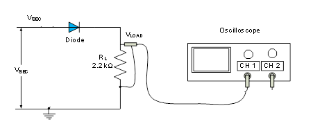
- Using the voltage VSEC obtained from the simulation, build the circuit in Figure 1 on the breadboard with VSEC as an input, which connects to the diode and load resistor RL in series. (See Figure 3)
- Using the jumper wires, screw driver and screw terminal connector, connect the board to NI MyDAQ Instrument Device to analyze the circuit.
- Use channel AO0 on the NI myDAQ Instrument Device to provide the input (VSEC) and channel AI0 to measure the output voltage(VLOAD).
- Using the function generator from NI ELVISmx Instrument Launcher, provide the input voltage VSEC to the circuit. Measure the output voltage VLOAD, across the load RL using the oscilloscope.
- Repeat steps 3 and 4 with a 100uF capacitor if you notice any variations in the output.
Figure 2
Review questions:
- What is the urpose of having a half-wave rectifier in the circuit?
- Describe the procedure in this lab to arrive at the final design of both the hardware portion and the software portion to achieve the design objectives?
- Discuss the impact of having the capacitor on the output voltage and the effect of additional load on the ripple voltage.
Deliverables:
- Measured voltage VSEC, the output peak voltage, VLOAD and ripple voltage VRIPPLE. Capture screenshots of your measurements from Multisim.
- Place your student ID card on the breadboard and take a picture of the circuit board and pin out on the NI myDAQ device.
- Take screenshots of the measurements obtained from function generator and oscilloscope on the NI ELVISmx Instrument Launcher on your screen.
Part B: Full wave rectification:
Software (Multisim):
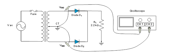
- Construct the circuit of a half-wave rectifier in Figure 3 in Multisim. Use a function generator to provide the AC input of Vacand use a center tapped transformer to obtain VSEC. Notice that the ground for the circuit has changed. Check your circuit carefully before applying power.
- Connect the Tektronix oscilloscope so that each channel is across each diode. Observe the waveforms VSEC across each diode and then observe the VLOAD.
- Connect a 100 μF capacitor (C1) with a tolerance of 20% in parallel with the load resistor (RL). (Note the polarity of the capacitor).
- Measure the dc load voltage, VLOAD, and the peak-to-peak ripple voltage, VRIPPLE, of the output. Measure the ripple frequency. Tabulate all data gathered and compare the results with and without the filter capacitor.
Figure 3
Hardware (NI myDAQ):
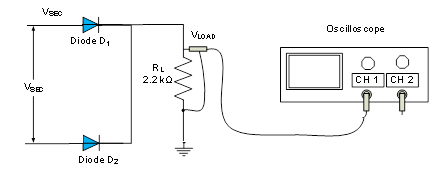
- Using twice the voltage VSEC obtained from the simulation, build the circuit in Figure 3 on the breadboard with 2*VSEC as an input, which connects to the two diodes and load resistor RL in series. (See Figure 4)
- Using the jumper wires, screw driver and screw terminal connector, connect the board to NI MyDAQ Instrument Device to analyze the circuit.
- Use channel AO0 on the NI myDAQ Instrument Device to provide the input (2*VSEC) and channel AI0 to measure the output voltage (VLOAD).
- Using the function generator from NI ELVISmx Instrument Launcher, provide the input voltage VSEC to the circuit. Measure the output voltage VLOAD, across the load RL using the oscilloscope.
- Repeat steps 3 and 4 with a 100uF capacitor if you notice any variations in the output.
Figure 4
Review questions:
- What is the purpose of having a full-wave rectifier in the circuit?
- Describe the procedure in this lab to arrive at the final design of both the hardware portion and the software portion to achieve the design objectives?
- Discuss the impact of having the capacitor on the output voltage and the effect of additional load on the ripple voltage.
- How is the output of the full-wave rectifier different from half-wave rectifier?
Deliverables:
- Measured voltage VSEC, the output peak voltage, VLOAD and ripple voltage VRIPPLE. Capture screenshots of your measurements from Multisim.
- Place your student ID card on the breadboard and take a picture of the circuit board and pin out on the NI myDAQ device.
- Capture screenshots of your measurements from the NI ELVISmx Instrument Launcher showing both the input from the function generator and output on the oscilloscope on your screen.
Lab Report:
- Use the Lab report template found in the “Tools and Template” link in the navigation center.
- Include all the deliverables from Part A and Part B.
- Include all the screenshots of the measurements from Multisim, circuit design on the breadboard using NI myDAQ device and measurements from MI ELVISmx Instrument Launcher.
- Save the document as Lab2YourGID.docx (ex: Lab2G00050331.docx) and submit in Blackboard.
Grading Rubrics
Grading CriteriaPointsPart A: Half-wave rectifier circuit in Multisim – with and without filter capacitor10Part A: Half-wave rectifier circuit on NI myDAQ and breadboard with and without filter capacitor10Part A: Deliverables: Measurements and screen captures from Multisim and hardware15Review Questions10Part B: Full-wave rectifier circuit in Multisim – with and without filter capacitor10Part B: Full -wave rectifier circuit on NI myDAQ and breadboard with and without filter capacitor10Part B: Deliverables: Measurements and screen captures from Multisim and hardware15Review Questions10Report format (Proper use of template)10TOTAL100